Band Structures
If the periodic potential V(\mathbf r) is known, it would be possible to solve the one-electron Schrödinger equation:
-\frac{\hbar^2}{2m} \nabla^2 \psi(\mathbf r) + \frac{\mathrm d^2}{\mathrm dx^2} + V(\mathbf r) \psi(\mathbf r) = E \psi(\mathbf r)
for which a solution in Bloch form:
\psi(\mathbf r) = u(\mathbf r)e^{-i \mathbf k \cdot \mathbf r}
where u(\mathbf r) is the same for each cell and e^{-i \mathbf k \cdot \mathbf r} is a propagating wave for a discrete set of allowed \mathbf k.
Calculating all the possible energies for all the k values gives a band structure; to compute the potential there are many method, but a common one is to make a model and then refine the shape of V(\mathbf r) based on experimental results.
Using bigger and bigger crystal (so that the are more and more k available) a graph can be progressively constructed: it is a set of points but, if there are many points, it can be represented with a continuous line.

The number of k-states in a band is equal to the number of unit cells in the crystal; there are many bands in general, but only a few are usually are important for determining the properties of the material, and in general only values which goes from \frac{\pi}{a} to \frac{\pi}{a} are plotted, what which is referred as the first Brillouin zone), for larger k the bands just repeat itself, furthermore the band is symmetric around x=0 (Kramers degeneracy).
This can be proven time reversing the Schrödinger equation, and it demonstrate that states with a spin at \mathbf k and the spin at - \mathbf k have the same values.
both semiconductors and insulators typically have a full valence band at absolute zero temperature. The key difference between them lies in their respective band gaps and how easily electrons in the valence band can be excited to the conduction band:
- In semiconductors, the band gap is small enough (typically 0.1 to 2\, eV) that at room temperature, thermal energy is sufficient to excite some electrons from the full valence band to the conduction band, allowing for electrical conductivity.
- In insulators, the band gap (generally greater than 4\, eV) is so large that very few, if any, electrons can be thermally excited to the conduction band under normal conditions, resulting in poor electrical conductivity.
- In metals the conduction bands is partially filled or overlapping conduction and valence bands, allowing free movement of electrons. This structure results in high electrical conductivity.
It worth noting that not only an empty conduction band does not conduct electricity (as there are not electrons to move) but also a full band neither (as there electrons cannot change their motion).
Semiconductor doping involves intentionally introducing impurities into an intrinsic (pure) semiconductor to modify its electrical properties, primarily to enhance its conductivity. The process involves adding a small amount of dopant atoms to the semiconductor crystal lattice. There are two types of doping:
-
N-type Doping:
- Dopant: Elements with more valence electrons than the semiconductor, typically from group V of the periodic table (like phosphorus, arsenic, or antimony for silicon-based semiconductors).
- Effect: These dopants have one more electron than needed to form the tetrahedral bonds typical in silicon lattices. The extra electron is loosely bound to its parent dopant atom and can easily move into the conduction band, thereby increasing the semiconductor’s electron concentration (negative charge carriers).
-
P-type Doping:
- Dopant: Elements with fewer valence electrons than the semiconductor, generally from group III of the periodic table (such as boron, aluminum, or gallium for silicon-based semiconductors).
- Effect: These dopants have one fewer electron for bonding with the surrounding silicon atoms, creating a “hole” in the lattice structure. This hole acts as a positive charge carrier, as neighboring electrons can move to fill the hole, effectively allowing the hole to move through the lattice.
N-type dopants introduce discrete energy levels near the conduction band, while P-type dopants introduce levels near the valence band. This makes it easier for electrons to be excited into the conduction band (N-type) or for holes to be created in the valence band (P-type).
Both types of doping increase the material’s conductivity by increasing the number of free charge carriers (electrons in N-type, holes in P-type).
The creation of regions within a semiconductor that are doped differently (N-type and P-type) is fundamental to the operation of devices like diodes and transistors. Junctions between different types of doped regions (PN junctions) are critical for controlling the flow of electrons and holes, enabling the switching and amplification functions of electronic components.
By carefully controlling the type and amount of doping, manufacturers can tailor the electrical properties of semiconductors for specific applications in electronic and optoelectronic devices.
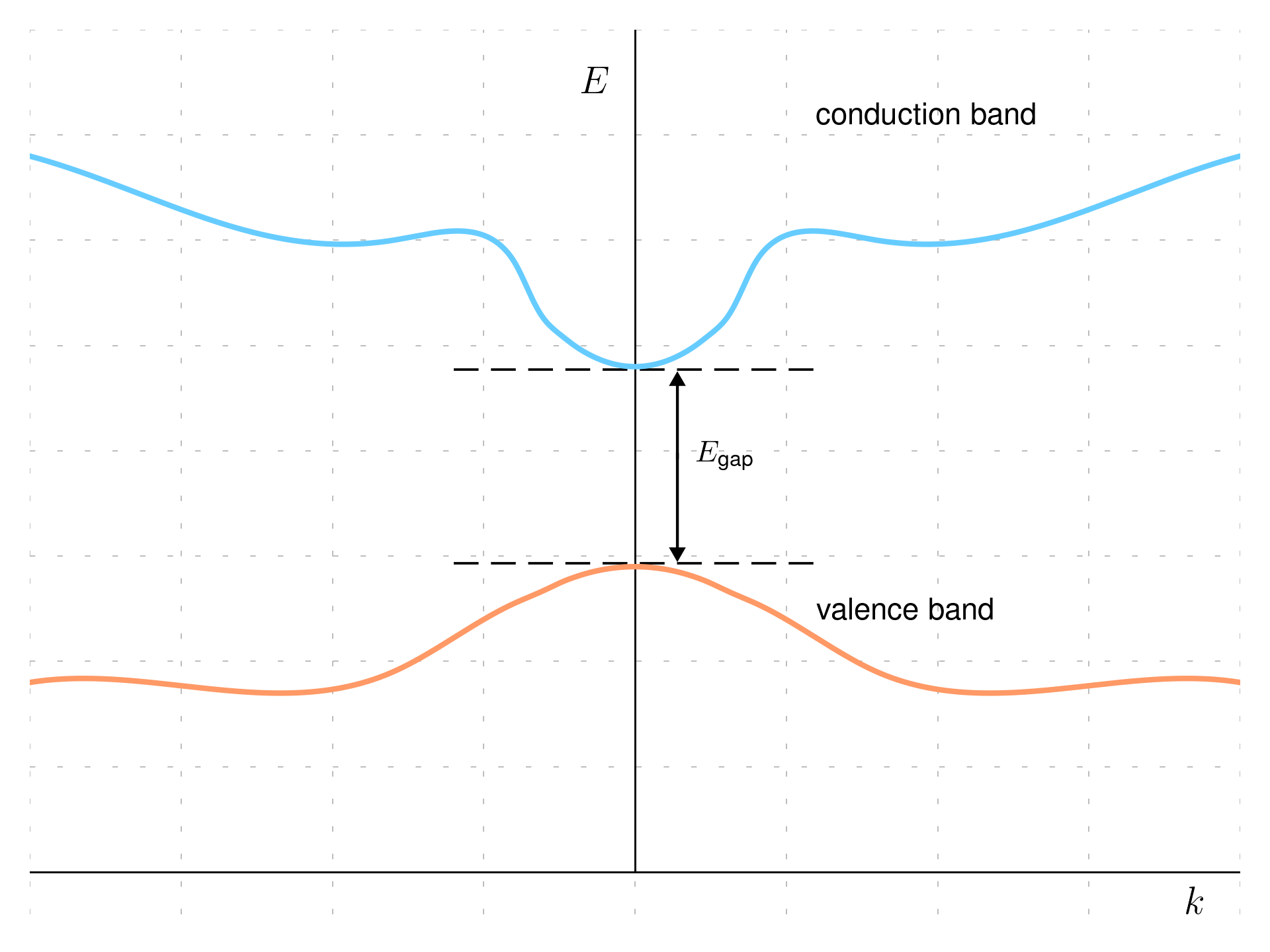
If the maximum of the valence band and the minimum of the conduction band occur at the same momentum (k-value) in the Brillouin zone, the semiconductor is called direct gap semiconductor. Electrons can move directly from the valence band to the conduction band without changing their momentum. This direct transition allows for efficient absorption and emission of light, making direct-gap semiconductors ideal for optoelectronic devices such as LEDs and laser diodes. The previous picture show an example of the band structure.

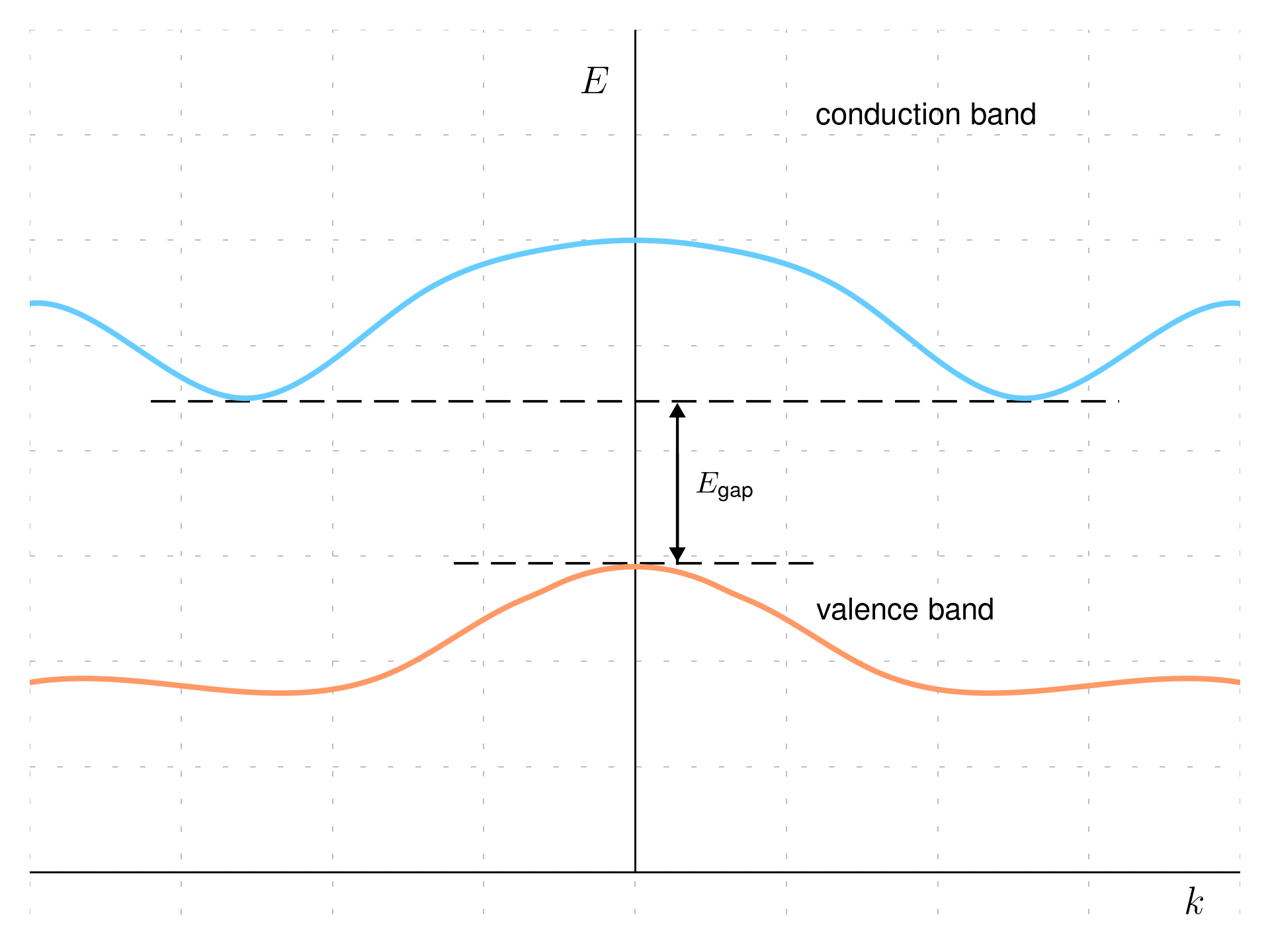
If the maximum of the valence band and the minimum of the conduction band occur at different momentum values, the semiconductor is called indirect gap semiconductor. Transitions between these bands require a change in momentum and therefore, indirect-gap semiconductors are less efficient at absorbing and emitting light compared to direct-gap semiconductors. This characteristic makes them less suitable for light-emitting applications but still useful in applications where light emission is not a critical factor, such as in certain types of photovoltaic cells and transistors.
Materials like gallium arsenide (GaAs) and cadmium telluride (CdTe) are example of direct-gap semiconductors, while silicon and germanium are examples of indirect-gap semiconductors.
The distinction between direct and indirect band gaps is critical in determining the suitability of semiconductor materials for various electronic and photonic devices. Direct-gap materials are predominantly used in devices that interact with light, while indirect-gap materials are commonly used in electronic applications where their properties can be advantageously employed despite their inefficiencies in light interaction.
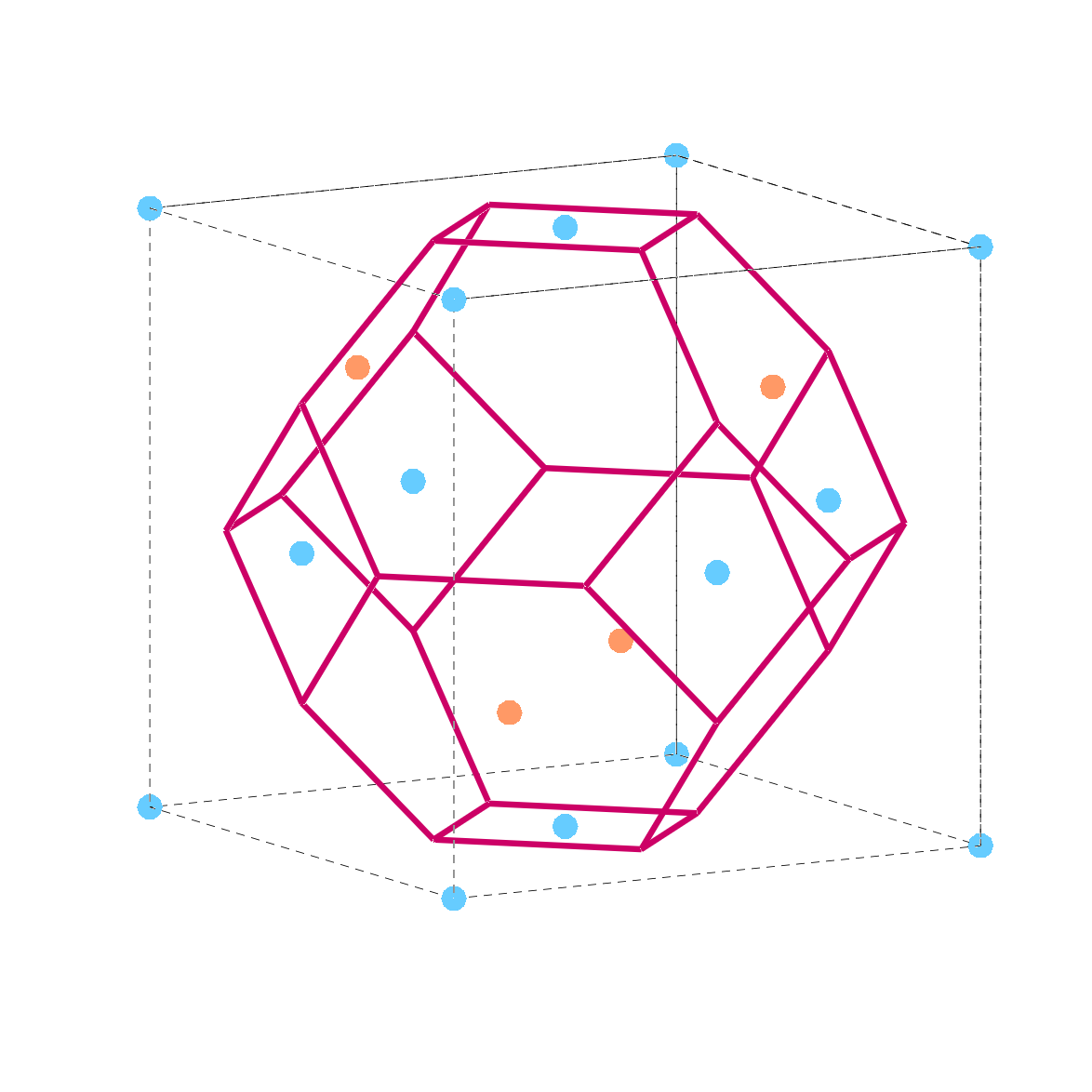
For 3D objects the situation is more complex; for example for the Zinc-blend it would look like in k space, like the red frame in the picture below (the size of the atoms has been made smaller to make the picture clearer).

Two important directions are the X direction and the L direction:
- The X point in the Brillouin zone of a zinc blende structure corresponds to the midpoint of the face of the cubic unit cell along the <100> direction. If considering the conventional cubic unit cell axes, where each axis (x, y, z) represents a primary crystallographic direction, the X point would be along any of the Cartesian axes extending from the origin to the face of the cube.
- The L point refers to a point along the <111> direction. This is the direction pointing from one corner of the cubic cell toward the opposite face’s center. Physically, visualizing the cube, this direction runs diagonally from one corner of the cube (where all three coordinates are either all zeros or all ones) through the body center of the cube and to the opposite corner.
- The center of Brillouin zone is called the Gamma point \Gamma.
To graphically visualize the band structure it is possible to plot it along direction of interest (for example the X and L directions starting from \Gamma) each one on an half of the graph because by Kramers degeneracy the other half will be the same.